
The Dissolution of the Fabless Model
The semiconductor industry is currently defined by the separation of design and manufacture. For decades, the fabless model enabled titans like NVIDIA and Apple to innovate rapidly by offloading the Herculean task of silicon fabrication to foundries like TSMC. Elon Musk’s Terafab project threatens to overturn this equilibrium. By earmarking $119 billion to internalize chip production, Musk is signaling that the era of relying on third-party foundries for essential high-performance silicon is reaching its expiration date.
In an environment where advanced AI models and robotics require hyper-specific hardware configurations, the one-size-fits-all approach of commercial foundry production creates a performance bottleneck. Musk’s pivot suggests that for a diversified technology conglomerate, dependency on external supply chains is no longer a logistical hurdle; it is a critical competitive weakness.
Vertical Integration as an AI Catalyst
Terafab is defined by its core objective: treating compute capacity as a proprietary utility. By integrating hardware architecture directly into the product R&D cycle—specifically for Tesla’s FSD stack and the Optimus robot—Musk aims to eliminate the translation layer between silicon designers and software engineers.
Collaborating with legacy players like Intel may provide the necessary technical scaffolding, but the end goal is a closed-loop system. When hardware is designed in tandem with neural network architectures, the innovation cycle compresses significantly. Companies forced to adhere to the rigid roadmaps of third-party foundries will inevitably trail behind those that can iterate on silicon at the same pace they update their software.
Compute Architecture as a Primary Economic Driver
Musk’s strategy rests on the assumption that compute power is the modern equivalent of 20th-century industrial electricity. If global economic growth is increasingly tied to the volume and speed of processed intelligence, then physical control over the infrastructure that generates that intelligence is the ultimate, non-replicable moat.
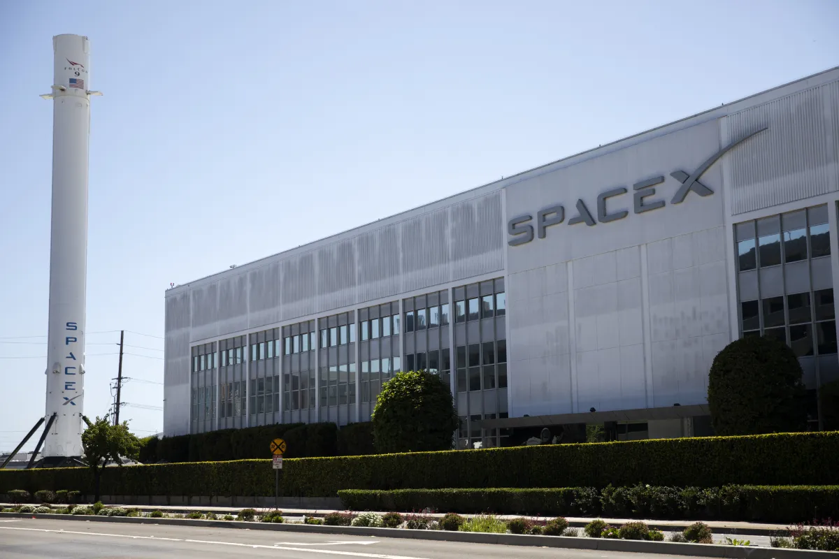
This move also serves as a hedge against the growing instability of global semiconductor supply chains. Geopolitical tensions centered on Taiwan and other fabrication hubs have created an environment of systemic risk. By repatriating fabrication, Musk is decoupling his product roadmaps from foreign trade volatility. Furthermore, envisioning a future where high-density compute, supported by reliable aerospace logistics, creates a decentralized processing network indicates a long-term plan to transcend the limitations of traditional, geography-locked data centers.
The Daunting Reality of Semiconductor Autarky
Despite the strategic brilliance of the vision, the execution faces profound challenges. Semiconductor fabrication plants (fabs) are perhaps the most complex, energy-demanding, and resource-heavy industrial facilities ever conceived. Success requires not only massive capital allocation but also access to rare raw materials, a highly specialized multi-generational workforce, and immense electrical throughput.
The localization of these facilities, particularly in states like Texas, will likely involve high-stakes lobbying for infrastructure subsidies and energy grid prioritization. The massive $119 billion capital expenditure requirement raises questions about the financial durability of the initiative. However, if Terafab achieves operational efficiency, it will create an existential crisis for the rest of the tech industry.
Should silicon manufacturing be successfully internalized, incumbents will be forced to choose between massive capital outlays to replicate the Full-Stack Sovereign model or risk being left behind by competitors with total control over their hardware roadmap. Ultimately, Musk is attempting to redefine the semiconductor industry from an outsourcing market into a foundational pillar of corporate infrastructure.