
The Silicon Pivot: Quantum Motion Secures $160M to Standardize Quantum Manufacturing
Quantum Motion Ltd., a London-based pioneer in quantum architecture, has successfully finalized a $160 million Series C funding round. Led by DCVC and Kembara, this substantial capital injection arrives three years after the firm’s previous financing milestone. The funding signifies more than just a balance sheet boost; it marks a strategic endorsement of silicon-based quantum computing as the most viable path toward commercial scalability.
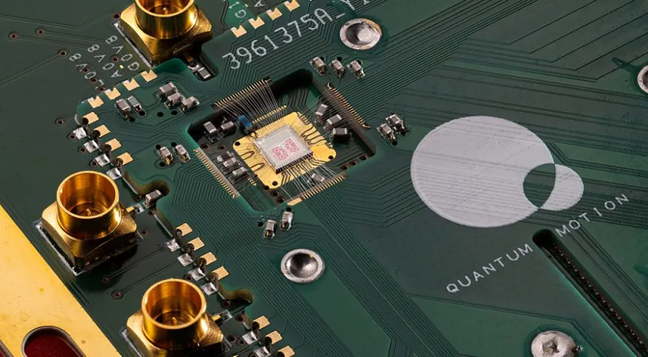
The company has already demonstrated technical viability by delivering a functional quantum computer to the UK National Quantum Computing Centre (NQCC). Spanning the volume of three standard server racks, the machine houses a processor measuring only a few millimeters—a sharp contrast to the room-sized, specialized cooling and cabling infrastructure typical of earlier-generation quantum hardware.
Beyond Exotic Materials: The CMOS Advantage
For years, the quantum industry has been fractured by competing hardware approaches, ranging from ion traps to complex photonic emitters. While these methods achieve impressive performance in laboratory settings, they often struggle with the manufacturing wall—the inherent difficulty of scaling production to thousands or millions of qubits.
Quantum Motion differentiates itself by leveraging existing CMOS (complementary metal-oxide-semiconductor) fabrication processes. By opting for silicon, the company bypasses the need for bespoke, proprietary manufacturing plants. This allows them to utilize the global ecosystem of semiconductor fabs, effectively piggybacking on decades of iterative progress in classical microchip production. If the hardware can be designed and simulated using standard industry software, the barrier to mass production drops significantly.
Architectural Convergence: Quantum Dots and Integrated Control
At the core of Quantum Motion’s strategy is a design philosophy that mirrors the evolution of the field-effect transistor (FET). Their processors utilize quantum dots—nanoscale semiconducting crystals—to trap individual electrons. By manipulating the spin states of these electrons, the system performs quantum computations.
A critical hurdle in quantum engineering has historically been the wiring bottleneck. Most quantum processors require massive arrays of coaxial cables to connect the cryogenic chips to room-temperature control electronics, leading to extreme heat leakage and space constraints.
Quantum Motion is tackling this by integrating the control circuitry directly onto the silicon die. By positioning the control logic in close proximity to the qubit architecture, the company eliminates the need for bulky external cabling. Furthermore, their proprietary Hoxton control chip utilizes super-inductors to achieve detection sensitivity roughly 100 times higher than conventional read-out systems.
Implications for the Data Center Ecosystem
The implications for the wider industry are significant. By reducing the physical footprint of quantum processors, Quantum Motion is theoretically positioning its hardware for integration into existing data center environments. In the past, the requirement for massive, custom-built, cryogenically cooled enclosures served as a deterrent for enterprise adoption.
By siliconizing the stack, Quantum Motion is moving quantum computing into the realm of commodity-style infrastructure. If their roadmap to exponentially increase qubit counts bears fruit, it could signal the end of the experimental phase of quantum hardware and the beginning of a true scaling era.
With this new $160 million runway, the focus for Quantum Motion will undoubtedly shift toward high-volume throughput. The objective is clear: moving from a boutique engineering project to a high-capacity production line that can prove silicon is not just a laboratory curiosity, but the bedrock of the next generation of computing.